Semiconductor Electronics: Materials, Devices and Simple Circuits – Physics Class 12 Notes
Chapter – 14
Semiconductor Electronics: Materials, Devices and Simple Circuits
1. Classification of Solids
On the basis of conductivity: metals (ρ ≈ 10-2 to 10-8 Ω m), semiconductors (ρ ≈ 10-5 to 106 Ω m) and insulators (ρ ≈ 1011 to 1019 Ω m). Semiconductors may be elemental (Si, Ge) or compound (GaAs, CdS, organic and polymer semiconductors).
Energy bands: in a crystal, the energy levels of the outer electrons of the many atoms spread into bands. The valence band contains valence electrons; the conduction band above it can hold electrons that are free to conduct. The gap between them is the energy band gap Eg.

Type | Band structure | Conduction |
|---|---|---|
Metal | Conduction and valence bands overlap, or the conduction band is partly filled | Many free electrons; conducts at all temperatures |
Semiconductor | Small gap, Eg < 3 eV (Si 1.1 eV, Ge 0.7 eV) | At 0 K an insulator; at room temperature some electrons cross the gap |
Insulator | Large gap, Eg > 3 eV (diamond about 5.4 eV) | Practically no conduction |
2. Intrinsic Semiconductors
A pure semiconductor (Si or Ge) is intrinsic. Each atom forms four covalent bonds with its neighbours. At room temperature, thermal energy breaks some bonds: an electron moves to the conduction band and leaves a vacancy called a hole (an effective positive charge) in the valence band. In an intrinsic semiconductor ne = nh = ni. Total current I = Ie + Ih. Electrons and holes also recombine continuously; at equilibrium the rate of generation equals the rate of recombination.
Numerical 1: Silicon has a band gap of 1.1 eV. Find the maximum wavelength of light that can create an electron-hole pair in it.
Given: Eg = 1.1 eV = 1.1 × 1.6 × 10-19 J
Formula: λmax = hc/Eg
Solution: λ = 6.63 × 10-34 × 3 × 108/(1.76 × 10-19) = 1.13 × 10⁻⁶ m
Answer: λmax ≈ 1130 nm (infrared)
3. Extrinsic Semiconductors
Adding a small amount of a suitable impurity (doping, about 1 part per million) greatly increases conductivity. The impurity (dopant) atom must be of nearly the same size as the host atom.

| n-type | p-type |
|---|---|---|
Dopant | Pentavalent (As, Sb, P): donor | Trivalent (B, Al, In): acceptor |
How carriers arise | The fifth valence electron is loosely bound and easily freed | The missing bond creates a hole that can accept an electron |
Energy level | Donor level just below the conduction band | Acceptor level just above the valence band |
Majority carriers | Electrons | Holes |
Minority carriers | Holes | Electrons |
Relation | ne ≫ nh | nh ≫ ne |
In both types the crystal remains electrically neutral. In thermal equilibrium, nenh = ni2.
Numerical 2: Pure Si has ni = 1.5 × 10¹⁶ m-3. It is doped with 4.5 × 10²² arsenic atoms per m3. Find the electron and hole concentrations.
Given: ni = 1.5 × 10¹⁶ m-3, ND = 4.5 × 10²² m-3; each As atom donates one electron
Formula: ne ≈ ND; nenh = ni2
Solution: ne ≈ 4.5 × 10²² m-3; nh = (1.5 × 10¹⁶)2/(4.5 × 1022) = 2.25 × 1032/4.5 × 1022
Answer: ne ≈ 4.5 × 10²² m-3; nh = 5 × 10⁹ m-3 (n-type)
Numerical 3: An n-type sample has ne = 1022 m-3 and ni = 1016 m-3. Find the ratio of majority to minority carriers.
Given: ne = 1022 m-3, ni = 1016 m-3
Formula: nh = ni2/ne
Solution: nh = 1032/1022 = 1010 m-3; ratio = 1022/1010
Answer: 1012 : 1
4. p-n Junction

When a p-region and an n-region are formed in a single crystal, two processes occur at the junction:
- Diffusion: holes diffuse from p to n and electrons from n to p because of the concentration difference, producing a diffusion current from p to n.
- This leaves behind immobile ions: negative acceptor ions on the p-side and positive donor ions on the n-side, forming a thin depletion region (about 10-6 m wide) with no free carriers.
- The ions create an electric field from n to p, which causes a drift current of minority carriers opposite to the diffusion current.
- At equilibrium, diffusion current = drift current and there is no net current. The potential difference across the depletion region is the barrier potential V0 (about 0.7 V for Si and 0.3 V for Ge).
5. Semiconductor Diode under Bias
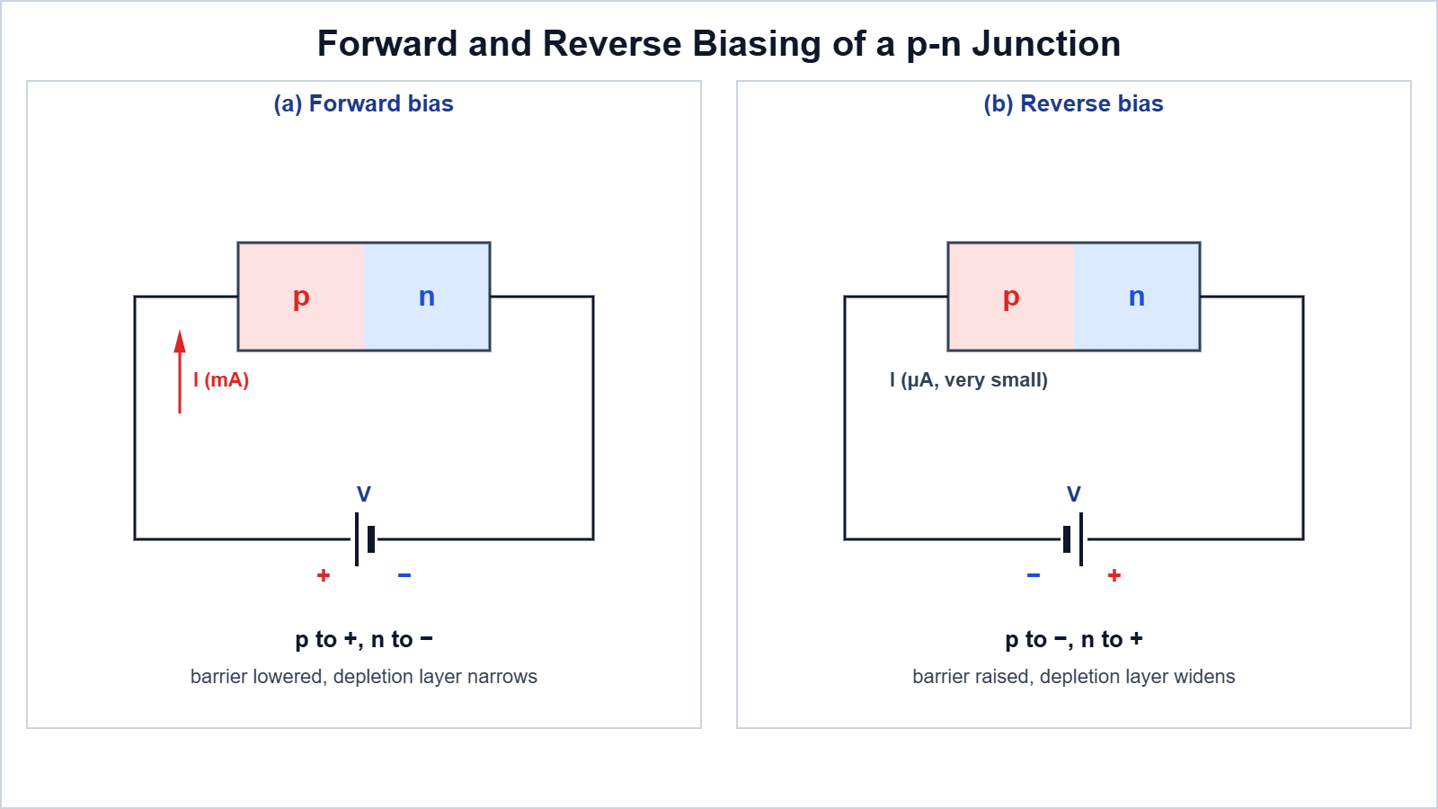
| Forward bias | Reverse bias |
|---|---|---|
Connection | p to positive, n to negative terminal | p to negative, n to positive terminal |
Barrier | Reduced to (V0 − V) | Increased to (V0 + V) |
Depletion layer | Narrows | Widens |
Current | Large (mA), due to majority carriers; rises sharply above the threshold (knee) voltage | Very small (μA), due to minority carriers; nearly constant (reverse saturation current) until breakdown |
Resistance | Low | Very high |

Dynamic resistance rd = ΔV/ΔI (the I-V graph is non-linear, so the diode is a non-ohmic device). Above the breakdown voltage in reverse bias the current rises sharply.
Numerical 4: A silicon diode (forward drop 0.7 V) is connected in series with a 430 Ω resistor across a 5 V battery in forward bias. Find the current.
Given: V = 5 V, VD = 0.7 V, R = 430 Ω
Formula: I = (V − VD)/R
Solution: I = (5 − 0.7)/430 = 4.3/430
Answer: I = 0.01 A = 10 mA
Numerical 5: When the forward voltage of a diode changes by 0.1 V, the current changes by 10 mA. Find its dynamic resistance.
Given: ΔV = 0.1 V, ΔI = 0.01 A
Formula: rd = ΔV/ΔI
Solution: rd = 0.1/0.01
Answer: rd = 10 Ω
6. Diode as a Rectifier
A rectifier converts AC into DC using the one-way conduction of a diode.

Half-wave rectifier: the diode conducts only during the half-cycles in which it is forward biased, so current flows through the load only in alternate half-cycles. The output is pulsating DC with the same frequency as the input (50 Hz for 50 Hz mains). Half of the input wave is wasted.

Full-wave rectifier (centre-tap): the secondary of a centre-tapped transformer gives two voltages in opposite phase to two diodes D1 and D2. In one half-cycle D1 is forward biased, in the next D2; current through the load is always in the same direction. Output frequency = 2 × input frequency (100 Hz for 50 Hz mains). It is more efficient than a half-wave rectifier.
Capacitor filter: a capacitor connected across the load charges to the peak voltage when the output rises and discharges slowly through the load when it falls, so the output is a nearly steady DC with a small ripple. A large C and a large RL (large time constant RLC) give a smoother output.
Numerical 6: The secondary of a transformer gives 12 V rms to a half-wave rectifier using a silicon diode. Find the peak output voltage (diode drop 0.7 V).
Given: Vrms = 12 V, VD = 0.7 V
Formula: Vpeak = √2 Vrms − VD
Solution: √2 × 12 = 16.97 V; 16.97 − 0.7
Answer: Vout(peak) ≈ 16.3 V (16.97 V for an ideal diode)
Numerical 7: The input to a rectifier is 50 Hz AC. Find the frequency of the output ripple for (i) a half-wave and (ii) a full-wave rectifier.
Given: fin = 50 Hz
Formula: Half-wave: fout = fin; full-wave: fout = 2fin
Solution: (i) 50 Hz; (ii) 2 × 50
Answer: (i) 50 Hz; (ii) 100 Hz
Exam point: In a full-wave rectifier each diode conducts for one half-cycle only, but the load receives current in both half-cycles.
Easy Memory Trick: “P to Positive = Pass”: connecting p to the positive terminal forward biases the diode and lets current pass.
7. Practice Numericals (Answers Only)
- A semiconductor has Eg = 3 eV. Find the longest wavelength it can absorb. Ans: about 414 nm.
- A full-wave rectifier is fed with 60 Hz AC. Find the output frequency. Ans: 120 Hz.
- A p-type sample has nh = 1020 m-3, ni = 1016 m-3. Find ne. Ans: 1012 m-3.
- An ideal diode is forward biased by 5 V through 1 kΩ. Find the current. Ans: 5 mA.
- What is the approximate barrier potential of a germanium junction? Ans: 0.3 V.
8. Board-pattern Practice Questions
(a) Multiple Choice Questions
1. In an n-type semiconductor the majority carriers are
(A) holes (B) electrons (C) protons (D) positive ions
Ans. (B)
2. The dopant used to make p-type silicon is
(A) arsenic (B) phosphorus (C) boron (D) antimony
Ans. (C)
3. In forward bias, the width of the depletion layer
(A) increases (B) decreases (C) remains same (D) becomes infinite
Ans. (B)
4. The output frequency of a full-wave rectifier for 50 Hz input is
(A) 25 Hz (B) 50 Hz (C) 100 Hz (D) 200 Hz
Ans. (C)
(b) Assertion-Reason
Options: (A) Both A and R are true and R is the correct explanation of A. (B) Both A and R are true but R is not the correct explanation of A. (C) A is true but R is false. (D) A is false but R is true.
1. Assertion (A): An n-type semiconductor is electrically neutral.
Reason (R): The extra electrons come from neutral donor atoms, which become positive ions.
Ans. (A)
2. Assertion (A): The reverse current of a diode is very small.
Reason (R): It is due to minority carriers, whose number is small.
Ans. (A)
(c) Match the Columns
Column I | Column II |
|---|---|
(i) Donor impurity | (p) Valence band and conduction band overlap |
(ii) Acceptor impurity | (q) Indium |
(iii) Metal | (r) Antimony |
(iv) Insulator | (s) Eg > 3 eV |
Ans. (i)-(r), (ii)-(q), (iii)-(p), (iv)-(s)
(d) Case Study
Case: Mobile phone chargers convert 220 V AC mains into about 5 V DC. Inside, the voltage is first stepped down, then rectified by diodes and smoothed by capacitors before being regulated.
(i) Which device changes AC to DC?
Ans. A rectifier (diodes).
(ii) Why is a full-wave rectifier preferred?
Ans. It uses both half-cycles, giving higher efficiency and less ripple.
(iii) What is the role of the capacitor?
Ans. It smooths the pulsating DC by charging at peaks and discharging between them.
(iv) How does increasing C affect the ripple?
Ans. The ripple decreases (larger time constant).
(e) Long Answer Questions
Q1. Explain the formation of the depletion region and barrier potential in a p-n junction. Draw and explain the I-V characteristics of a diode in forward and reverse bias.
Ans. See Sections 4 and 5.
Q2. With a circuit diagram and waveforms, explain the working of a full-wave rectifier. How is its output smoothed?
Ans. See Section 6.
9. Important Questions
Q1. What is a hole?
Ans. A vacancy of an electron in a covalent bond, acting as a positive charge carrier.
Q2. Write the relation between ne, nh and ni.
Ans. nenh = ni2.
Q3. Why is a semiconductor an insulator at 0 K?
Ans. No electrons have enough energy to cross into the conduction band.
Q4. Name the two processes at a p-n junction.
Ans. Diffusion and drift.
Q5. What is the depletion region?
Ans. A region near the junction without free charge carriers, containing immobile ions.
Q6. What is the barrier potential of a silicon junction?
Ans. About 0.7 V.
Q7. Why is a diode called a non-ohmic device?
Ans. Its I-V graph is non-linear and depends on the direction of voltage.
Q8. What is the output frequency of a half-wave rectifier for 50 Hz input?
Ans. 50 Hz.
Q9. What happens to resistivity of a semiconductor when temperature increases?
Ans. It decreases.
Q10. What is dynamic resistance?
Ans. rd = ΔV/ΔI at a point on the I-V characteristic.
Conclusion: Band theory explains the difference between metals, semiconductors and insulators. Doping produces n-type and p-type materials; their junction forms a diode, whose one-way conduction is used in half-wave and full-wave rectifiers.